Chip Design with Deep Reinforcement Learning
April 23, 2020
Posted by Anna Goldie, Senior Software Engineer and Azalia Mirhoseini, Senior Research Scientist, Google Research, Brain Team
Quick links
Update, June 9, 2021: Today in Nature, we've published methods that improve on what is discussed below, and that have been used in production to design the next generation of Google TPUs.
The revolution of modern computing has been largely enabled by remarkable advances in computer systems and hardware. With the slowing of Moore’s Law and Dennard scaling, the world is moving toward specialized hardware to meet the exponentially growing demand for compute. However, today’s chips take years to design, resulting in the need to speculate about how to optimize the next generation of chips for the machine learning (ML) models of 2-5 years from now. Dramatically shortening the chip design cycle would allow hardware to adapt to the rapidly advancing field of ML. What if ML itself could provide the means to shorten the chip design cycle, creating a more integrated relationship between hardware and ML, with each fueling advances in the other?
In “Chip Placement with Deep Reinforcement Learning”, we pose chip placement as a reinforcement learning (RL) problem, where we train an agent (i.e, an RL policy) to optimize the quality of chip placements. Unlike prior methods, our approach has the ability to learn from past experience and improve over time. In particular, as we train over a greater number of chip blocks, our method becomes better at rapidly generating optimized placements for previously unseen chip blocks. Whereas existing baselines require human experts in the loop and take several weeks to generate, our method can generate placements in under six hours that outperform or match their manually designed counterparts. While we show that we can generate optimized placements for Google accelerator chips (TPUs), our methods are applicable to any kind of chip (ASIC).
The Chip Floorplanning Problem
A computer chip is divided into dozens of blocks, each of which is an individual module, such as a memory subsystem, compute unit, or control logic system. These blocks can be described by a netlist, a graph of circuit components, such as macros (memory components) and standard cells (logic gates like NAND, NOR, and XOR), all of which are connected by wires. Determining the layout of a chip block, a process called chip floorplanning, is one of the most complex and time-consuming stages of the chip design process and involves placing the netlist onto a chip canvas (a 2D grid), such that power, performance, and area (PPA) are minimized, while adhering to constraints on density and routing congestion. Despite decades of research on this topic, it is still necessary for human experts to iterate for weeks to produce solutions that meet multi-faceted design criteria. This problem’s complexity arises from the size of the netlist graph (millions to billions of nodes), the granularity of the grid onto which that graph must be placed, and the exorbitant cost of computing the true target metrics, which can take many hours (sometimes over a day) using industry-standard electronic design automation tools.
The Deep Reinforcement Learning Model
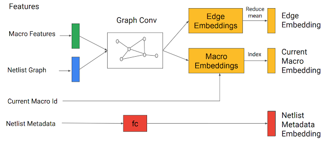
The input to our model is the chip netlist (node types and graph adjacency information), the ID of the current node to be placed, and some netlist metadata, such as the total number of wires, macros, and standard cell clusters. The netlist graph and the current node are passed through an edge-based graph neural network that we developed to encode the input state. This generates embeddings of the partially placed graph and the candidate node.
 |
| A graph neural network generates embeddings that are concatenated with the metadata embeddings to form the input to the policy and value networks. |
In each iteration of training, the macros are sequentially placed by the RL agent, after which the standard cell clusters are placed by a force-directed method, which models the circuit as a system of springs to minimize wirelength. RL training is guided by a fast-but-approximate reward signal calculated for each of the agent’s chip placements using the weighted average of approximate wirelength (i.e., the half-perimeter wirelength, HPWL) and approximate congestion (the fraction of routing resources consumed by the placed netlist).
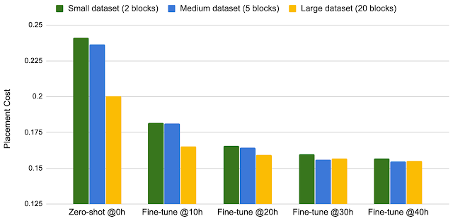
To our knowledge, this method is the first chip placement approach that has the ability to generalize, meaning that it can leverage what it has learned while placing previous netlists to generate better placements for new unseen netlists. We show that as we increase the number of chip netlists on which we perform pre-training (i.e., as our method becomes more experienced in placement optimization), our policy better generalizes to new netlists.
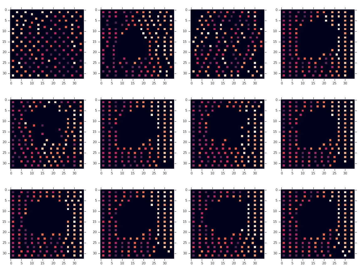
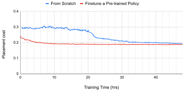
For example, the pre-trained policy organically identifies an arrangement that places the macros near the edges of the chip with a convex space in the center in which to place the standard cells. This results in lower wirelength between the macros and standard cells without introducing excessive routing congestion. In contrast, the policy trained from scratch starts with random placements and takes much longer to converge to a high-quality solution, rediscovering the need to leave an opening in the center of the chip canvas. This is demonstrated in the animation below.
 |
| Macro placements of Ariane, an open-source RISC-V processor, as training progresses. On the left, the policy is being trained from scratch, and on the right, a pre-trained policy is being fine-tuned for this chip. Each rectangle represents an individual macro placement. Notice how the cavity discovered by the from-scratch policy is already present from the outset in the pre-trained policy’s placement. |
 |
| Convergence plots for two policies on Ariane blocks. One is training from scratch and the other is finetuning a pre-trained policy. |
 |
| Training data size vs. fine-tuning performance. |
Acknowledgements
This project was a collaboration between Google Research and Google Hardware and Architecture teams. We would like to thank our coauthors: Mustafa Yazgan, Joe Jiang, Ebrahim Songhori, Shen Wang, Young-Joon Lee, Eric Johnson, Omkar Pathak, Sungmin Bae, Azade Nazi, Jiwoo Pak, Andy Tong, Kavya Srinivasa, William Hang, Emre Tuncer, Anand Babu, Quoc Le, James Laudon, Roger Carpenter, Richard Ho, and Jeff Dean for their support and contributions to this work.
Quick links
×
❮
❯


